

How Southeast Quartz Empowers Wafer Fab Yield as a China Premium Quartz Wafer Carrier Factory
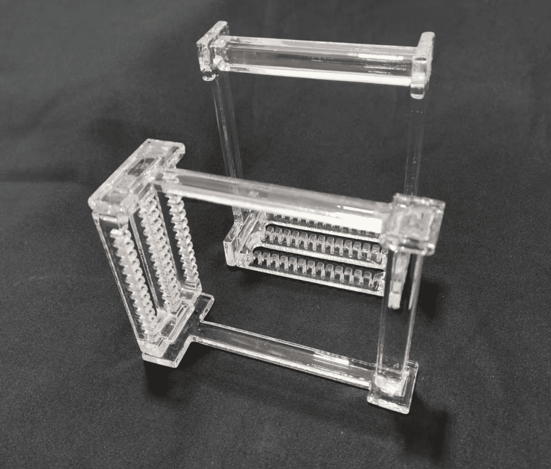

The Hidden Yield Risks of Conventional Quartz Carriers
During advanced thermal treatments, structural consumables remain in direct contact with silicon wafers. Conventional quartz boats frequently contain microscopic vulnerabilities invisible to the naked eye. If a carrier features high surface roughness along its internal slots or retains internal stresses from inadequate thermal treatment, it becomes a continuous processing risk. Micro-fissures and rough interior surfaces trap particulate matter or residues. In a high-temperature furnace, these trapped micro-particles detach and settle onto the wafer, causing severe patterning defects or surface contamination after chemical-mechanical planarization.
Furthermore, standard industrial-grade quartz often carries minute structural impurities. Under prolonged exposure to working temperatures exceeding 1100 degrees Celsius, trace elements like sodium, potassium, or iron migrate out of the quartz matrix. This outgassing allows metallic ions to diffuse into active silicon layers, leading to localized gate oxide breakdown and early component failure. By approaching yield management through material purity and structural precision, Southeast Quartz provides semiconductor facilities with a reliable method to suppress these hidden contamination vectors.
Key Physical Attributes Influencing Carrier Performance
To eliminate contamination risks during critical wafer processing phases, technical teams must analyze three primary physical attributes of any quartz transport assembly.
1.Base Material Purity and Composition
The chemical composition of the fused silica substrate determines its long-term inertness under extreme thermal loads. To function effectively in semiconductor environments, the base material must exhibit a silicon dioxide content equal to or greater than 99.99 percent. Restricting trace alkali metals to less than 10 parts per million prevents the thermal diffusion of mobile ions into delicate silicon structures. Maintaining this chemical purity ensures that the quartz structural component does not interact with processing gases or outgas volatile metallic elements during prolonged operations.
2.Surface Characteristics and Passivation
The physical texture of the inner walls where the silicon wafer rests governs the accumulation of microscopic particulates. High surface roughness increases the total surface area available for chemical adsorption, making the carrier difficult to clean. Controlling the surface roughness value and applying specialized hydrofluoric acid passivation treatments helps eliminate surface micro-voids and micro-fractures. This precise surface finishing suppresses devitrification成核点 (crystallization nuclei), reducing the risk of material flaking during repetitive thermal cycles.
3.Structural Geometries and Machine Alignment
Modern automated wafer fabrication lines rely on high-precision robotic arms to load and unload wafers into quartz slots. Any dimensional variance in slot pitch, slot depth, or the positioning of alignment pins can cause minor mechanical interference during transfer. Even microscopic friction between the wafer edge and an misaligned quartz slot can generate structural micro-scratches and silicon dust. Precise dimensional matching across all structural features ensures smooth robotic handling and minimizes mechanical stress on the wafer edges.
Advanced Production Controls at Southeast Quartz
Lianyungang Southeast Quartz Products Co., Ltd. operates from Donghai County, Lianyungang City, Jiangsu Province—a recognized national base for the silicon material industry. This geographic positioning grants the enterprise direct access to high-quality natural quartz ore resources, establishing a consistent supply chain for high-purity raw materials. To convert these resources into functional semiconductor-grade components, the factory integrates advanced technological infrastructure with strict quality management protocols.
The production cycle utilizes specialized computer numerical control cutting and milling systems operating under continuous fluid cooling. This advanced machining capability allows Southeast Quartz to achieve exceptional dimensional tolerances, restricting slot geometry variations to within plus or minus 0.05 millimeters. Following the initial mechanical profiling, skilled technicians employ automated oxy-hydrogen flame polishing systems to melt away surface micro-fissures and achieve a smooth, uniform surface texture.
To eliminate residual thermal stresses introduced during cutting and welding, completed carriers undergo a multi-stage thermal annealing process in computer-controlled ovens. This stress-relief sequence prevents structural warping or cracking when the component encounters rapid temperature fluctuations during service. Finally, every batch undergoes chemical cleaning and inspection within Class 100 or Class 1000 cleanroom environments. Each shipment from the quartz wafer carrier factory includes a dedicated purity analysis statement and full dimensional verification records, providing complete traceability for facility quality audits.
Process Adaptation and Validation Frameworks
Different phases of semiconductor manufacturing subject quartz carriers to distinct physical environments, requiring tailored material configurations to maximize operational lifetimes.
High-Temperature Diffusion and Oxidation: Vertical and horizontal furnace operations require multi-layer quartz boats engineered to withstand continuous operating temperatures above 1100 degrees Celsius. For these applications, Southeast Quartz focuses on maximizing material density and thermal shock resistance, preventing structural deformation during long-term thermal cycling.
Wet Chemical Cleaning and Storage: Transport cassettes and open-style carriers used in chemical etching and intermediate storage require exceptional chemical passivity. The manufacturing process optimizes surface smoothness and cleanroom packaging to prevent chemical retention and eliminate airborne particle collection.
To verify the operational benefits of premium consumables, engineering teams can implement a structured Design of Experiments framework. By running parallel production lots using standard carriers alongside advanced units from Southeast Quartz, process engineers can directly track post-cleaning particle counts, surface defect densities, and final parametric yield stability.
Protecting Yield Across Global Supply Chains
As semiconductor geometries continue to shrink, the impact of process consumables on overall manufacturing stability becomes more pronounced. Selecting an experienced fabrication partner allows semiconductor facilities to manage defect risks at the material source. Lianyungang Southeast Quartz Products Co., Ltd. combines regional raw material advantages with precision engineering capabilities to supply dependable quartz solutions to international markets. Technical buyers and process engineers can submit specific wafer dimensions, ranging from 4-inch to 12-inch configurations, along with equipment model specifications and custom slot requirements, to secure compatible, high-purity components engineered to safeguard fabrication yield.
To discover more about the comprehensive product lines, material certifications, and custom manufacturing options, please visit the official corporate portal at https://www.dnquartz.com/
Lianyungang Southeast Quartz Products Co.,Ltd.
Lianyungang Southeast Quartz Products Co.,Ltd.
+86 135 8528 6180
email us here
Legal Disclaimer:
EIN Presswire provides this news content "as is" without warranty of any kind. We do not accept any responsibility or liability for the accuracy, content, images, videos, licenses, completeness, legality, or reliability of the information contained in this article. If you have any complaints or copyright issues related to this article, kindly contact the author above.
